Coupling light from standard 8.2 μm SMF-28e+ fiber into a reverse-tapered silicon waveguide on an erbium-doped photonic circuit requires matching mode sizes that differ by more than 3x — a mismatch that otherwise dumps most of the light as insertion loss.
Approach
Developed an HF wet-etching adiabatic taper process to narrow fiber tips from 8.2 μm down to 2.5 μm, built a room-temperature optical station to characterize the resulting taper profiles, and used Lumerical FDTD/MODE simulations to pre-screen taper geometries before committing them to the etch bench.
Outcome
Sub-0.1 dB coupling loss into the reverse-tapered waveguide, with simulation-guided pre-screening cutting design-iteration count by roughly 60%.
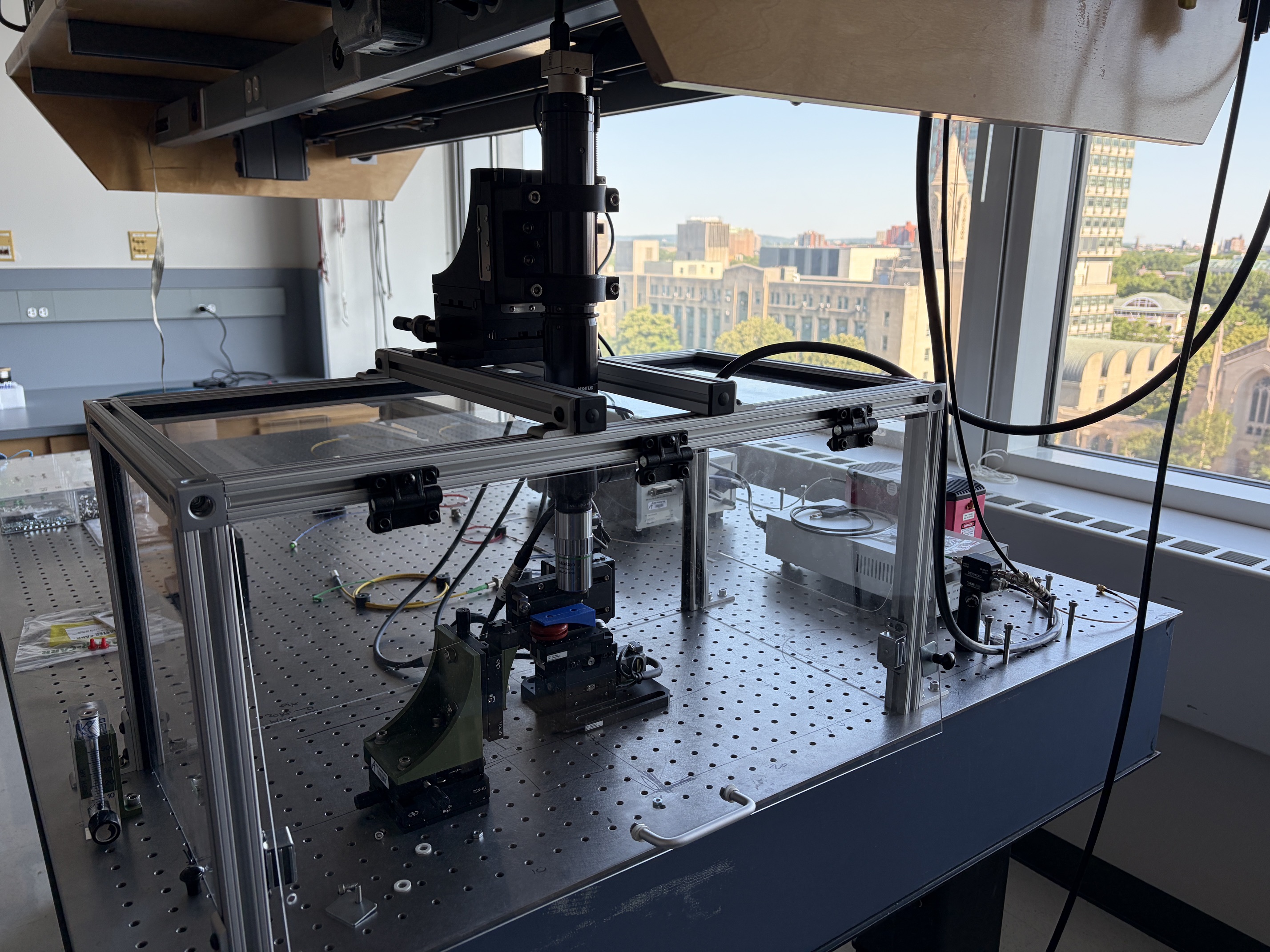
Fig. 1 — Room-temperature optical testing station used to characterize fiber taper profiles.
Overview
I work in the Lake Lab at Boston University, where we build photonic circuits on erbium-doped substrates for quantum applications. Getting light on and off those chips efficiently is its own hard problem: the chip-side waveguides are reverse-tapered down to a couple of microns, while the fiber that has to feed them is a standard 8.2 μm SMF-28e+ core. Left as-is, that size mismatch throws away most of the light before it ever reaches the circuit.
My work focuses on closing that gap on the fiber side — tapering the fiber tip down to match the waveguide's mode field, characterizing how well each taper couples, and using simulation to narrow down which taper geometries are worth fabricating in the first place.
Fiber tapering process
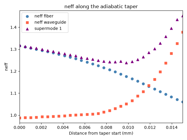
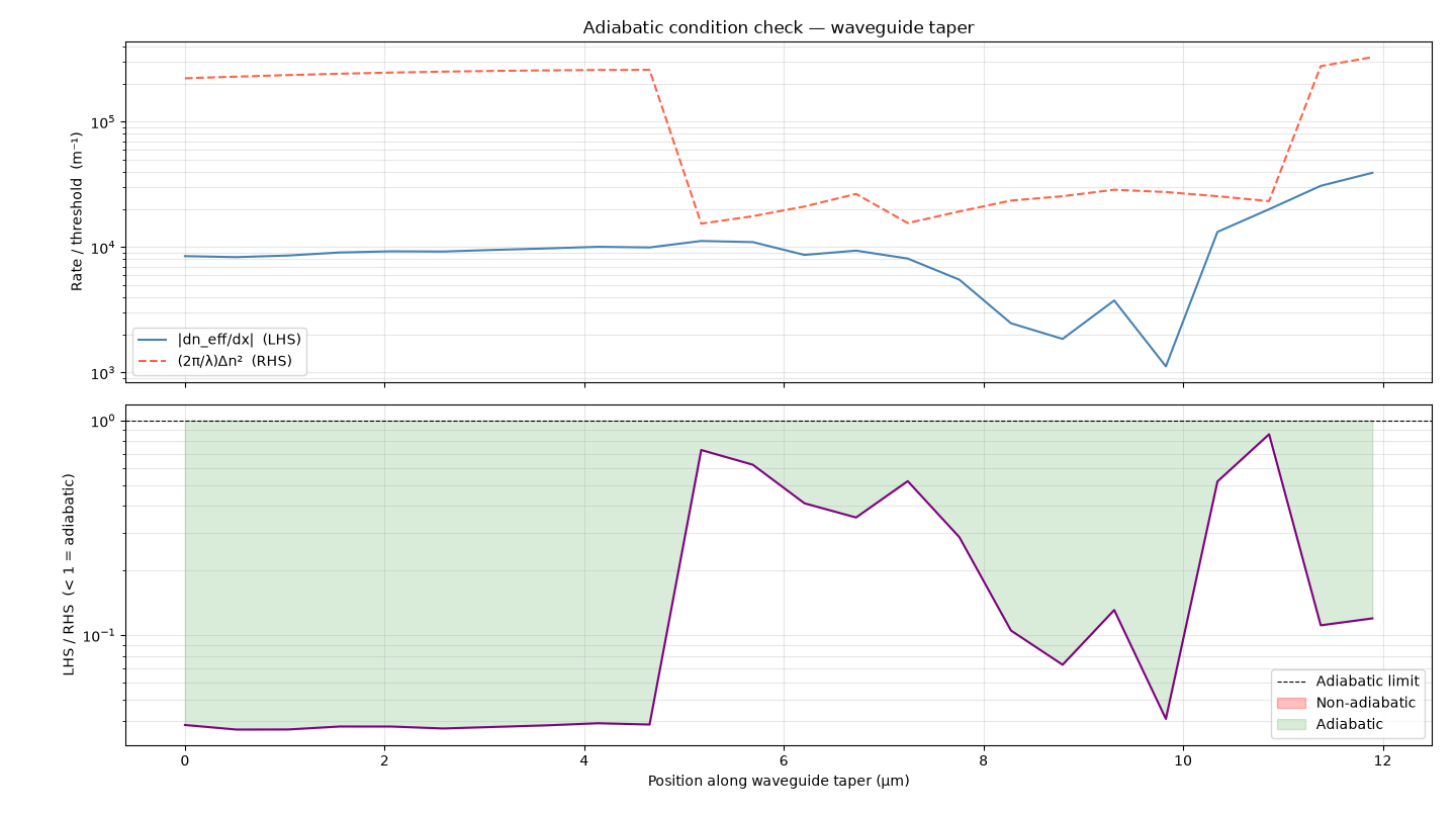
I developed an HF wet-etching adiabatic taper process that narrows the fiber from its native 8.2 μm core down to 2.5 μm at the tip. "Adiabatic" is the key constraint here — the taper has to shrink slowly enough that the guided mode stays confined the entire way down, instead of radiating out into the cladding partway through. Get the etch profile wrong and coupling efficiency collapses even if the final tip diameter is correct.
Tuned correctly, this process gets sub-0.1 dB coupling loss into the reverse-tapered silicon waveguide, which then feeds into the erbium-doped photonic circuit.
Fig. 2 — Effective index of each mode along the taper length.
Fig. 3 — Adiabaticity check: local mode-coupling rate vs. threshold.
Optical characterization station
To actually know whether a given taper etch worked, I built a room-temperature optical testing station from off-the-shelf components — fiber launch, alignment stages, and detection — that lets me pull a taper profile and measure its coupling efficiency quickly, without needing to book time on shared cryogenic or cleanroom equipment for every measurement. That turnaround is what makes it practical to iterate on etch parameters at all.
Simulation-guided design
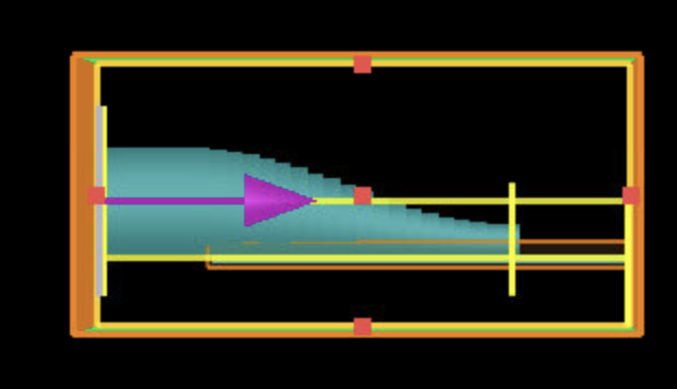
Before committing a taper geometry to the etch bench, I model it in ANSYS Lumerical using FDTD and MODE solvers to estimate coupling efficiency against the target waveguide mode. Pre-screening candidate geometries this way — rather than etching and measuring every variant — cut the number of physical design iterations by roughly 60%.
Simulation graphs
FDTD simulation geometry — source and monitors around the taper region.
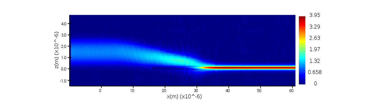
Field propagation through the taper, x–z cross-section.
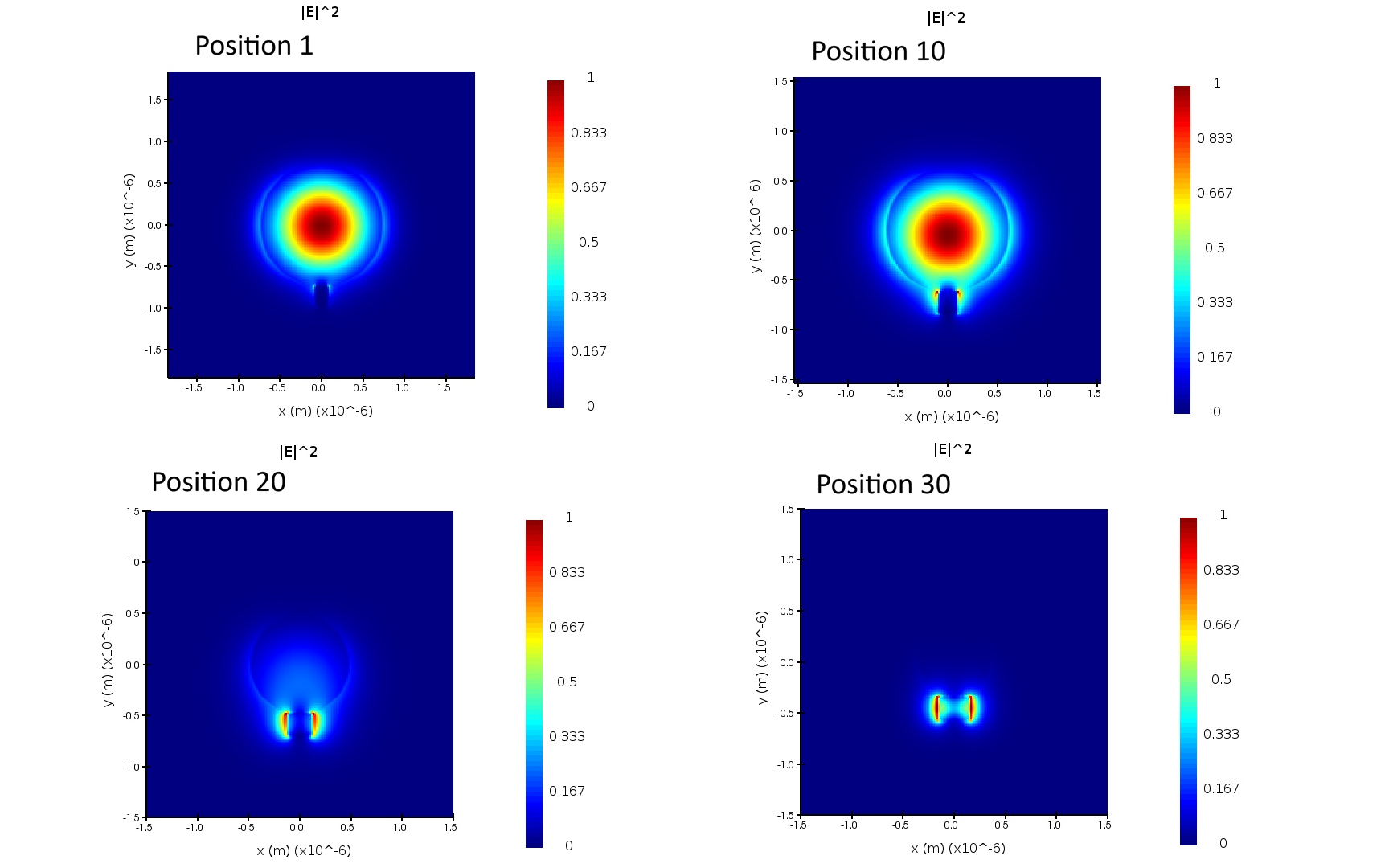
Mode profile (|E|²) evolution across four taper cross-sections.
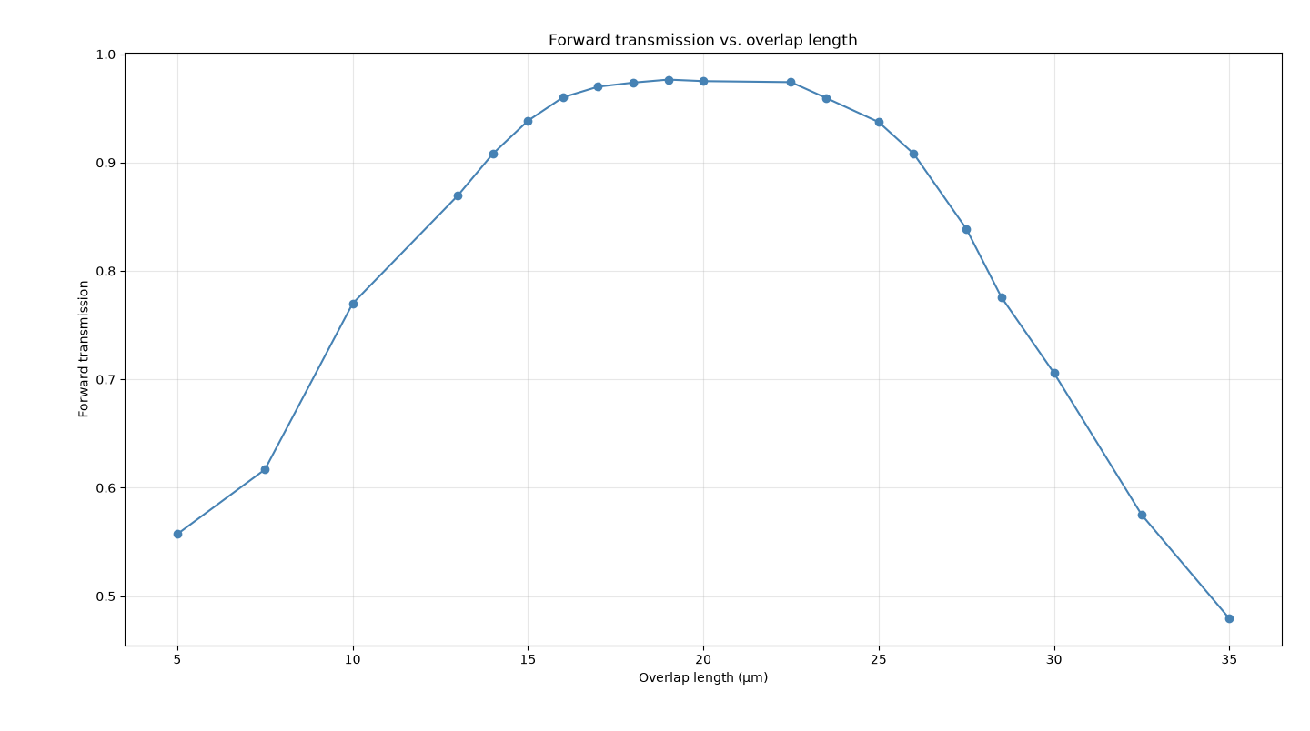
Transmission vs. overlap length — the kind of sweep used to pre-screen geometries before fabrication.